

 Product
 Brand
Brand Articles
 Tools
Tools
CAN FD Transceiver Selection Guide: Loop Delay, Bus Faults, and Low-Power Architecture
Upgrading a Controller Area Network from classic CAN 2.0 to CAN FD compresses the data-phase bit budget from() down to() or() [1, 5]. At these speeds, physical layer propagation delays and edge asymmetry—not raw microcontroller clock speeds—govern communication stability [1, 2].
A successful transceiver selection strategy rests on five interdependent physical layer parameters:
Total Loop Delay (): Must remain low across operating temperatures (typically, against the ISO 11898-2 ceiling of 255 ns[2]) [1, 2].
Loop Delay Symmetry (): Dictates received bit distortion at remote nodes regardless of microcontroller delay compensation [2, 5].
Continuous DC Bus Fault Voltage (): Must survive direct harness shorts to battery or DC bus lines (±42 V to ±70 V[4]) without degradation [2, 4].
Unpowered Bus Impedance (): Must remain high-impedance to prevent unpowered nodes from loading active buses through internal clamping diodes [1, 3].
Logic Level Interfacing (): Must match low-voltage microcontroller I/O (to) directly, eliminating external level-shifter propagation delay and jitter [2].
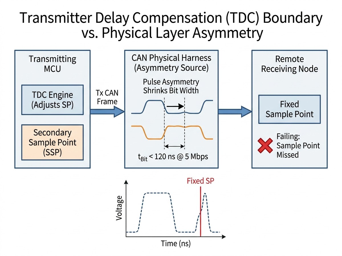
A critical architectural rule governs this selection: Transmitter Delay Compensation (TDC) inside the microcontroller CAN controller only protects the transmitting node's internal bit check; it cannot correct physical pulse asymmetry delivered to remote receiving nodes [2, 5].
1. Executive Decision Framework: The CAN FD Selection Model
Selecting a CAN FD transceiver requires stepping through three architectural criteria before finalizing a bill of materials (BOM):
Step 1: System Rail & Fault Environment
12 V Automotive (Passenger Cars): Requiresshort tolerance.
24 V Commercial / Heavy-Duty / Equipment: Requiresshort tolerance.
48 V Mild-Hybrid / Industrial Power Stages: Requiresshort tolerance.
Step 2: Low-Power & Network Sleep Architecture
Always-on or locally switched node: Standard standby mode.
Battery-backed sleep with remote bus wake: ISO 11898-2 Wake-up Pattern (WUP)[7] (,filtering).
Step 3: Network Topology & Data Phase Speed
Short backplane (< 5 m) or point-to-point: Standard ISO 11898-2:2016 (up to).
Multi-drop distributed harness (2 Mbps): Standard ISO 11898-2:2016 ().
Complex multi-drop topology (≥ 2–5 Mbps): CAN SIC (Signal Improvement Capability / CiA 601-4 / ISO 11898-2:2024).
Engineering Decision Rules
The Voltage Rail Check: Match continuous DC fault tolerance to the worst-case continuous short-circuit rail in the wiring bundle (e.g., dual-battery jump-starts in 24V commercial systems reach 36V to 48V; 48V mild-hybrid rails experience continuous overvoltage conditions up to 58V–70V) [2, 4].
The Thermal De-rating Rule: Never qualify a transceiver based on typicalloop delay. Propagation delay and pulse asymmetry widen significantly at high junction temperatures (AEC-Q100 Grade 1/0) [2, 7].
The Second-Source Rule: Pin-compatible SOIC-8 or DFN-8 transceivers must match not justand pinout, but loop delay symmetry windows () and unpowered leakage (I_OFF)[1] [1, 2, 6]. Divergent symmetry between alternate sources can induce sporadic bit errors at high temperatures in production [2].
2. Physical Layer Timing Physics: Loop Delay, Asymmetry, and the Controller TDC Boundary
Total Loop Delay () Anatomy
Total loop delay represents the round-trip propagation time through the transceiver physical layer:
: The delay from the microcontroller pulling
TXDlow to the driver producing a differential dominant voltage () acrossCANHandCANL[1, 2].: The delay from the differential bus crossing the receiver threshold () to the transceiver pulling
RXDlow [1, 2].
Under ISO 11898-2:2016, the standardized maximum ceiling foriswhen loaded by,, and[2]. While this upper ceiling sufficed for classic 1 Mbps CAN (where a bit interval is), it consumes excessive timing margin at higher speeds [1, 5]. Modern high-speed CAN FD transceivers typically restrictto betweenandacross temperature [1, 2].
The Physics of Loop Delay Asymmetry ()
During arbitration, transceivers operate ator, where transition asymmetries represent a negligible percentage of the bit budget [1, 5]. In the CAN FD data phase, this margin collapses [1, 5].
The asymmetry stems from fundamental circuit physics:
Dominant Transition: Actively driven by low-impedance push-pull internal MOSFETs driving
CANHhigh andCANLlow [1, 2].Recessive Transition: Completely passive. The driver transistors turn off, and the bus capacitance () discharges through the externaldifferential termination resistance () [1, 2].
Because active turn-on and passive turn-off rates differ, the propagation delay from recessive-to-dominant () rarely matches dominant-to-recessive () [2]. This imbalance shortens or widens the received recessive bit () [2, 6].
To maintain sampling integrity, ISO 11898-2:2016 (Clauses 5.6, Tables 13 and 14) establishes standardized received recessive bit width tolerances for standard bus test loads ():
| Data Rate | Nominal Transmit Bit Time () | Bus Bit Width () | Received Bit Width () | Receiver Timing Symmetry () |
|---|---|---|---|---|
| 2 Mbps | ||||
| 5 Mbps |
If passive bus discharge or transceiver silicon asymmetry widens dominant bits, the received recessive bit () shrinks belowat[2]. When this occurs, remote receiving nodes whose sample points are configured near 70%–80% of the nominal bit time will sample dominant voltage during a recessive bit window, triggering a bit or stuff error [2, 5].
The Controller vs. Transceiver Boundary: Demystifying TDC
Microcontroller datasheets frequently emphasize hardware Transmitter Delay Compensation (TDC), leading some hardware designers to conclude that transceiver loop delay and symmetry are no longer critical constraints [5]. This represents an architectural misunderstanding.
What Controller TDC Does
During the fast data phase, bit duration (at) is frequently shorter than the total round-trip physical delay () [2, 5].
Under classic CAN rules, a transmitter samples its own RXD line at its standard sample point inside the transmitted bit to verify bus state [5]. If round-trip delay exceeds:
(whereis Data Phase Time Segment 1), the transmitted bit has not returned to RXD by the sample point [5]. Without compensation, the transmitter detects a mismatch between TXD and RXD and generates a false bit error [5].
To resolve this, the CAN FD controller TDC engine measures physical loop delay using a hardware delay counter on the TXD-to-RXD edge transition [5]. It dynamically configures a Secondary Sample Point (SSP) offset by the measured delay plus a configurable register offset () as defined in the CAN FD Controller Module reference architecture[5] [5]. This allows the controller to self-check bits transmitted two or more clock periods earlier without raising false bit errors [5].
What Controller TDC Cannot Do
TDC operates strictly within the transmitting microcontroller's internal digital logic [5]. It does not modify the analog differential edges driven onto the copper wiring harness [2, 5].
If a transceiver exhibits poor loop delay symmetry (), recessive bits contract across the physical harness [2, 6]. Remote receiving nodes on the network do not use TDC for frame reception; they sample incoming data at a fixed nominal or data-phase sample point synchronized to frame transitions [5]. If the received bit width shrinks beyond the timing margin, remote nodes will mis-sample the bit, emit an active error frame, and corrupt communication [2, 5].
Selecting a transceiver with verified ISO 11898-2:2016 symmetry timing is mandatory to ensure interoperability across remote receivers, regardless of controller TDC capabilities [2, 6].
3. Electrical Survivability & Low-Power States: Bus Faults, Ground Offsets, and WUP
DC Bus Fault Survivability vs. Operational Common-Mode Range
Designers frequently confuse absolute maximum DC bus fault ratings with operational common-mode voltage range [2, 4]:
DC Bus Fault Voltage (Absolute Maximum): The maximum continuous direct-current voltage that can be applied to
CANHorCANLwith respect to local ground without causing dielectric breakdown, latch-up, or permanent hardware failure [1, 2].Operational Common-Mode Range (): The electrical boundary (defined by ISO 11898-2 as, extended in advanced automotive transceivers to) within which the differential receiver can reject common-mode offset and accurately decode valid differential data () [1, 2].
| System Environment | Operating Supply | Typical DC Short Risk | Recommended DC Bus Fault Rating | Recommended Common-Mode Range |
|---|---|---|---|---|
| 12 V Automotive (Passenger Cars) | Nominal (Oper.) | Direct short tobattery rail; load dumps up to. | Continuous | Standard |
| 24 V Commercial / Heavy Vehicles | Nominal (Oper.) | Dual battery jump-start (); severe load dump surges. | Continuous | Extended |
| 48 V Mild-Hybrid / Industrial DC Bus | Nominal (Oper.) | Harness chaffing directly topower distribution rails. | Continuous | Extended |
Engineering Warning: A transceiver rated forbus fault protection will survive a continuous short to abattery line without hardware damage, but it cannot decode frames while the bus line remains shorted to, because that common-mode voltage exceeds the receiver's operational decoding window [2].
Low-Power Standby and Wake-up Pattern (WUP) Filtering
Battery-backed Electronic Control Units (ECUs)—such as body control modules, telematics gateways, and anti-theft systems—must remain in sub-sleep states when the vehicle is parked [7].
In basic transceivers, wake-up detection relies on an unfiltered dominant bus level [7]. In automotive environments, high-energy electromagnetic pulses, inductive motor de-energization, and ground bounce easily pull differential lines into a dominant state momentarily, causing false ECU wake-ups and parasitic battery drain [7].
To prevent false wakes, ISO 11898-2:2016 defines a standardized 3-event Wake-up Pattern (WUP):
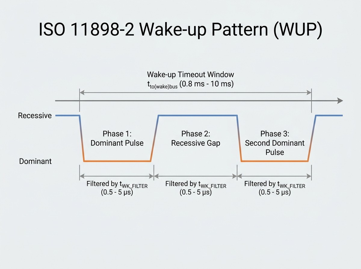
First Dominant Phase: Differential voltage must remain dominant continuously for at least() [7].
Intermediate Recessive Phase: Differential voltage must transition to recessive and remain for at least[7].
Second Dominant Phase: Differential voltage must transition back to dominant for at least[7].
All three events must occur within the wake-up timeout window (, typically) [7]. If bus noise produces a transientdominant pulse without the subsequent filtered recessive/dominant sequence, the transceiver logic rejects it, keeping the host microcontroller in sleep mode and holding standby currents below[7].
The Unpowered Node Parasitic Path ()
In partial-networking architectures, certain ECUs are depowered () to conserve energy while other nodes continue active communication across the shared bus [1, 6].
The Failure Mode: Standard integrated circuits feature electrostatic discharge (ESD) protection structures connected between internal pins and supply rails [1]. When, these diodes become forward-biased when an active transceiver drives
CANHto[1, 2].The Consequences:
Active bus signals are clamped down to the diode forward voltage (~), corrupting differential signaling across the network [1, 2].
The unpowered node pulls current from the bus, parasitically back-powering its ownrail and associated microcontroller peripherals [1].
The Solution: Transceivers must specify low unpowered pin leakage (I_OFF ≤ ±1 μA[6] or) across[1, 3]. Internal isolation circuits ensure input stages present a high-impedance state to
CANHandCANLwhen, preventing bus loading [1, 6].
4. Topology Realities vs. Vendor Myths: Harness Physics, Logic Rails, and High-Speed Limits
Dispelling the "5 Mbps Across the Harness" Fallacy
Transceiver marketing collateral often features claims of "5 Mbps" or "8 Mbps" operation [1, 3]. Hardware engineers must not assume these data rates function over long, branched vehicle harnesses [1, 8].
The physical constraints governing maximum bitrate are determined by transmission line physics:
Harness Propagation Delay: Signals travel down automotive twisted-pair copper cable at approximately
(
) [8]. On a
harness, the two-way round-trip cable delay alone is:
At
, the total nominal bit time is only
[2]. The cable propagation delay alone exceeds the entire bit time, rendering standard arbitration and round-trip feedback topologies unviable at that length [2, 8].
Stub Reflections and Ringing: Industrial and automotive networks often use untuned drop lines (stubs) to connect distributed nodes [8]. When a transceiver transitions from dominant to recessive, the transmission line discontinuity at an un-terminated stub reflects energy back onto the main trunk [8].
To prevent reflections from corrupting data, critical un-terminated stub lengths must satisfy:
In practice, this requires keeping un-terminated stubs belowin high-speed systems [8].
On complex networks with multiple stubs, ringing extends well into thebit window, crossing receiver thresholds and causing bit errors [2, 8]. As a result, standard ISO 11898-2:2016 CAN FD is realistically bounded toon distributed topologies [2, 8]. Achievingrequires point-to-point links, backplanes under, or transceivers equipped with Signal Improvement Capability (CAN SIC / CiA 601-4 / ISO 11898-2:2024) such as the TCAN857-Q1 CAN SIC transceiver[3], which actively damp ringing during recessive transitions [3, 8].
Logic Level Integration: Dedicatedvs. Discrete Level Shifters
Modern microcontrollers operate with digital I/O banks biased ator[1, 2]. However, CAN transceivers require asupply rail onto generate the ISO-standard dominant differential bus voltage () [1, 2].
Attempting to resolve this with external discrete level shifters (e.g., dual-supply bidirectional translation buffers) introduces significant design risks:
Discrete level shifters introduceof additional propagation delay into both the transmit and receive paths.
Unequal high-to-low and low-to-high translation times introduce external pulse skew, degrading the transceiver's loop delay symmetry before signals reach the physical bus [2].
Increased component count consumes board space and adds failure points.
Transceivers with an integrated(or) pin solve this by internally powering the digital input (TXD, STB) and output (RXD) buffers from the microcontroller's I/O rail () while powering the analog bus driver from[2, 6, 7]. This maintains tightly matched internal timing margins [2].
Mixed-Voltage Bus Compatibility (vs.Nodes)
Engineers frequently ask whether single-rail-powered CAN transceivers can communicate with standard-powered transceivers on the same physical wiring harness [1, 2].
The answer is yes, provided the 3.3V transceiver complies with ISO 11898-2 differential specifications [1, 2].
CAN is a differential protocol:
Recessive State:[1, 2].
Dominant State:(typically) [1, 2].
While atransceiver biases its recessive common-mode level to(), complianttransceivers generate a dominant differential voltage () with a lower common-mode bias (~) [1, 2]. Because CAN differential receivers decodeover an operational common-mode window of at least, both transceiver types interoperate reliably without signal corruption [1, 2].
5. Comparative Transceiver Matrix and Selection Trade-offs
The following table provides verified parametric specifications across representative automotive and industrial CAN FD transceivers:
| Part Number | Manufacturer | Max Data Rate | Typ / Max Loop Delay () | DC Bus Fault Voltage () | Common-Mode Range () | Standby Current () | Logic Supply | Automotive Qual | Primary Target Application |
|---|---|---|---|---|---|---|---|---|---|
| TCAN332G [1] | Texas Instruments | 5 Mbps | N/A (Standard) | None (Rail Only) | Industrial / Select Auto | Single-railspace-constrained designs | |||
| TCAN1042HV [2] | Texas Instruments | 5 Mbps | Low-Power Standby | DedicatedPin | AEC-Q100 Grade 1 | harsh automotive power buses | |||
| TCAN857-Q1 [3] | Texas Instruments | 5 Mbps | Low-Power Standby | DedicatedPin | ISO 11898-2:2024 / Q100 | Emerging CAN SIC / high-speed multi-drop buses | |||
| ISO1042-Q1 [4] | Texas Instruments | 5 Mbps | N/A (Isolated) | Dedicated Side-1 Rail | AEC-Q100 Grade 1 | High-voltage EV traction inverters, BMS, solar | |||
| TJF1051 [6] | NXP Semiconductors | 5 Mbps | Silent / Off Mode | DedicatedPin | AEC-Q100 Grade 1 | General automotive body and chassis control | |||
| TLE9252V [7] | Infineon Technologies | 5 Mbps | (WUP Filtered) | DedicatedPin | AEC-Q100 / VeLIO | Ultra-low-power battery-tied automotive ECUs |
Architectural Trade-off Analysis
Ultra-Low Delay vs. Radiated EMI: Transceivers featuring faster loop delays () utilize high slew-rate output stages [1, 2]. While this sharpens timing margins, it can increase high-frequency common-mode emissions [2]. High-speed designs typically require an external common-mode choke () to pass automotive CISPR 25 Class 5 conducted and radiated emissions limits.
Extreme Fault Protection vs. Capacitive Loading: Transceivers providingfault survivability integrate larger internal high-voltage DMOS protection structures [2, 4]. These structures introduce higher parasitic pin capacitance on
CANHandCANL(~) than non-protected components, which slightly reduces the maximum allowable node count on distributed networks [2].Galvanic Isolation vs. Latency Budget: Galvanically isolated transceivers (e.g., ISO1042-Q1) incorporate high-voltage capacitive or magnetic isolation barriers [4]. These barriers introduce an extraof internal propagation delay [4]. While necessary for operator safety and ground isolation inEV battery management systems, this added latency requires larger phase buffer segments in MCU bit timing configurations [4, 5].
6. Board-Level Bring-Up, Oscilloscope Verification, and Lab Checklist
Oscilloscope Verification Setup forand Symmetry
Accurate measurement of sub-150 ns propagation delays and bit symmetry requires proper probing techniques and standardized bus loading [1, 2]:
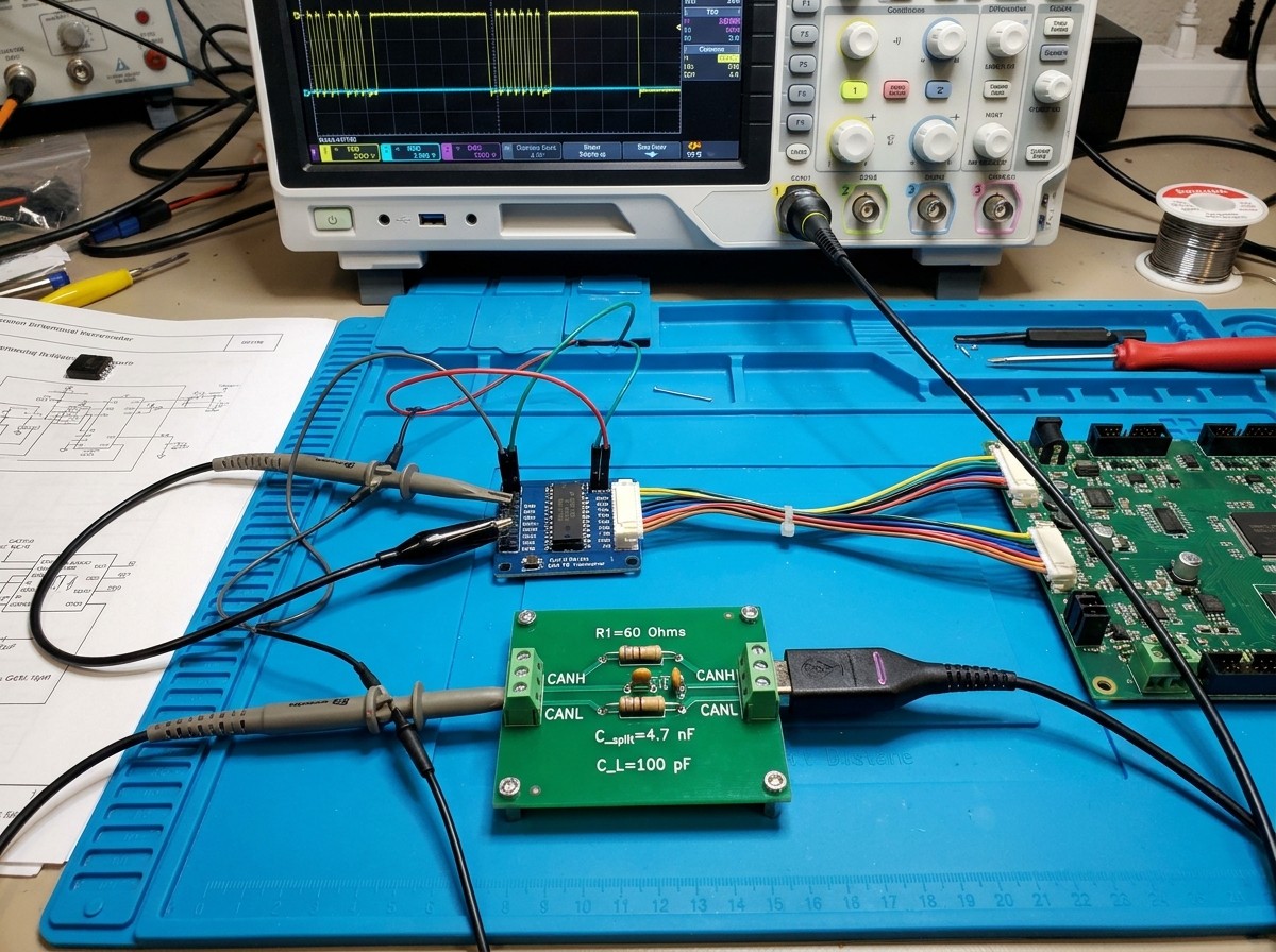
Standard Load Fixture: Terminate the transceiver with a split-termination network: twometal film resistors ($0.1\%$) in series with acommon-mode capacitor tied from their center tap to ground. Connect a lumpedlow-inductance ceramic capacitor between
CANHandCANLto simulate standard harness capacitance [2].Probe Calibration: Use high-bandwidth active single-ended probes (, input capacitance) for
TXDandRXD. Standard passiveprobes with long ground leads introduce inductive ground ringing that will invalidate sub-200 ns timing measurements. Use a calibrated differential probe acrossCANHandCANL[2].Loop Delay Measurement: Set the oscilloscope to trigger on the falling edge of
TXDat the 50% voltage threshold (on asystem). Measure the time delta () to the corresponding 50% falling edge onRXD[2]. This is[2]. Repeat for the rising edge to determine[2].Received Bit Symmetry () Measurement: Transmit a bitstream containing alternating bits (
10101010) and single recessive bits surrounded by dominant bits at the target data phase rate (or) [2]. Measure the pulse width of the recessive bit onRXDat the 50% logic threshold [2]. Verify that the measured width falls within the ISO 11898-2:2016 limits (for 2 Mbps;for 5 Mbps) [2].
FDCAN External Loop-back Mode
Pre-Hardware Firmware Validation: FDCAN Loopback Modes
Microcontroller peripherals (e.g., STM32 FDCAN, TI MCAN) provide internal and external loopback modes to validate protocol software prior to PCB assembly:
Internal Loopback Mode: The CAN core disconnects its receive engine from the physical
FDCAN_RXpin and forces the physicalFDCAN_TXpin to hold a continuous recessive state (). Transmitted bits route directly from the transmit shift register to the receive shift register internally. This mode enables developers to verify Message RAM allocation, FIFO handling, and Bitrate Switching (BRS) firmware without placing signal transitions onto an active harness.External Loopback Mode: The peripheral routes its transmit engine back to its receive engine internally, but also continues driving the physical
FDCAN_TXpin. This enables developers to probe the physical output pins and verify baud-rate prescalers and bit timing segment configurations using an oscilloscope, even before mounting external transceivers.
Practical Loopback Verification Traps
The "Scope Trap" on
RXD: During external loopback mode, the feedback from TX to RX occurs entirely within the microcontroller silicon. The physicalFDCAN_RXGPIO pin is disconnected from the receive engine. Probing theRXDpin will show a flatline, even while the firmware receives valid frames into its receive FIFO. Only the physicalTXDpin transitions.The ACK Masking Pitfall: In loopback modes, the CAN controller automatically acknowledges its own transmitted frames within the peripheral macro. The frame will succeed even if no partner node is attached and no termination resistors are present. Loopback modes do not validate bus loading, harness impedance, split termination, or partner transceiver ACK generation.
Hardware Bring-Up & Schematic Review Checklist
[ ] Bus Termination: Verifiedtotal bus termination (typically tworesistors with a centralcapacitor to ground for common-mode filtering).
[ ] Supply Rail Decoupling: Placed alow-ESR ceramic capacitor directly adjacent to thepin, accompanied by aceramic bulk capacitor.
[ ] Logic Level Alignment: If using a transceiver with apin, verified thatis tied directly to the microcontroller's I/O supply (or) and decoupled with acapacitor.
[ ] ESD and Transients: Placed bidirectional AEC-Q101 compliant ESD suppression diodes immediately adjacent to the board connector, ahead of the common-mode choke.
[ ] Common-Mode Choke (CMC): Placed a common-mode choke (or) between the ESD diodes and transceiver bus pins to suppress emissions without degrading differential edge rates.
[ ] Unpowered Bus Integrity (): Verified that the selected transceiver specifiesacrossif the node will be unpowered on an active network [1, 3].
[ ] DC Fault Safety Margin: Checked that the transceiver continuous DC fault withstand rating exceeds the highest voltage rail present in the harness bundle [2, 4].
7. Frequently Asked Questions (FAQ)
Does the Microchip MCP2515 stand-alone controller support CAN FD?
No. The MCP2515 is a legacy SPI controller that supports classic CAN 2.0B up to 1 Mbps only. It cannot parse the flexible data payload (up to 64 bytes) or bit-rate switching fields of CAN FD frames. Upgrading a design requires a CAN FD controller such as the MCP2517FD or MCP2518FD, or a microcontroller with integrated CAN FD hardware.
Can a classic CAN 2.0 transceiver be used in a CAN FD network operating at 2 Mbps?
No. While classic transceivers can physically transition fast enough to transmit 1 Mbps arbitration frames, they lack certified loop delay symmetry () specifications [2]. Their passive dominant-to-recessive transitions are not sufficiently controlled, causing recessive bits to shorten during 2 Mbps or 5 Mbps data phases [2]. Remote nodes will mis-sample these shortened bits and emit active error frames [2].
How does termination resistance tolerance affect loop delay and bit symmetry?
Because the dominant-to-recessive transition is passive, the bus discharge rate is determined by the $RC$ time constant formed by the differential termination resistance and lumped network capacitance:
If termination resistance increases (e.g., missing termination resistors, open traces, or degraded components),increases. The recessive discharge slows, extending the dominant-to-recessive delay and shrinking the received recessive bit width () [2].
What is the functional difference between CAN FD and CAN SIC transceivers?
Standard CAN FD transceivers (ISO 11898-2:2016) drive dominant states actively and rely entirely on external termination resistors to discharge the bus to recessive [1, 2]. On networks with long stubs, the impedance mismatches cause signal reflections (ringing) during recessive transitions [8].
CAN SIC transceivers (complying with CiA 601-4 and ISO 11898-2:2024) incorporate active circuitry that engages during recessive transitions to actively damp ringing on the bus [3, 8]. This suppresses reflections, preserves recessive bit widths, and allows data rates of 2 Mbps to 5 Mbps to operate reliably over complex, branched wiring harnesses without requiring point-to-point topologies [3, 8].
Sources and references used for this guide
TCAN332G 3.3-V CAN Transceivers with CAN FD Part Details
Source type: official company documentation
Used for: Loop delay specifications (<135 ns), 3.3V VCC operation, unpowered high-impedance pin behavior (IOFF), and operating temperature ranges.
Caution: Vendor product documentation; reflects performance under specific standard capacitive bus load conditions.TCAN1042 Fault Protected CAN Transceiver with CAN FD
Source type: official company documentation
Used for: DC bus fault protection voltage ratings up to ±70V, propagation delay symmetry, and automotive physical layer compliance.
Caution: Vendor datasheet; DC fault withstand voltage must not be confused with active common-mode operating range.TCAN857-Q1 Automotive Fault-Protected CAN FD Transceiver Datasheet
Source type: official company documentation
Used for: ISO 11898-2:2024 compliance details, advanced thermal shutdown, TXD dominant timeout, and high-voltage fault protection.
Caution: Vendor datasheet; references emerging ISO 11898-2:2024 standard which incorporates latest physical layer requirements.ISO1042 Isolated CAN Transceiver With 70-V Bus Fault Protection
Source type: official company documentation
Used for: Galvanic isolation architectures, 152 ns loop delay characteristics, and high-voltage industrial CAN FD survivability.
Caution: Specific to isolated transceiver architectures; isolation barriers introduce additional timing considerations compared to non-isolated transceivers.MCP25XXFD Family Reference Manual - CAN FD Controller Module
Source type: official company documentation
Used for: Transmitter Delay Compensation (TDC) mechanics, Secondary Sample Point (SSP) calculation, and controller bit-error boundary conditions.
Caution: Focuses on CAN controller digital IP registers and timing; must be distinguished from physical transceiver delay characteristics.TJF1051 High-Speed CAN Transceiver Datasheet
Source type: official company documentation
Used for: ISO 11898-2:2016 loop delay symmetry definitions, received bit width tolerances, and unpowered node behavior.
Caution: Vendor datasheet provided via authorized distributor document repository.TLE9252V Dual CAN FD Transceiver Technical Overview
Source type: official company documentation
Used for: ISO 11898-2:2016 compliant 5 Mbps loop delay symmetry, Wake-up Pattern (WUP) filtering times (0.5 µs to 5 µs), and standby modes.
Caution: Distributor catalog entry summarizing manufacturer technical datasheet specifications.TLE9351SJ High-Speed CAN FD Transceiver Datasheet Overview
Source type: official company documentation
Used for: VeLIO certification, SAE J2284-4/5 compliance, and 5 Mbps automotive loop delay symmetry.
Caution: Distributor summary; verify detailed switching waveforms directly against Infineon engineering specifications.
 UTMEL
UTMEL
We are the professional distributor of electronic components, providing a large variety of products to save you a lot of time, effort, and cost with our efficient self-customized service. careful order preparation fast delivery service
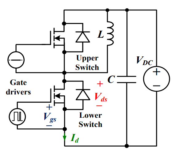 Discovering New and Advanced Methodology for Determining the Dynamic Characterization of Wide Bandgap DevicesSaumitra Jagdale15 March 20242843
For a long era, silicon has stood out as the primary material for fabricating electronic devices due to its affordability, moderate efficiency, and performance capabilities. Despite its widespread use, silicon faces several limitations that render it unsuitable for applications involving high power and elevated temperatures. As technological advancements continue and the industry demands enhanced efficiency from devices, these limitations become increasingly vivid. In the quest for electronic devices that are more potent, efficient, and compact, wide bandgap materials are emerging as a dominant player. Their superiority over silicon in crucial aspects such as efficiency, higher junction temperatures, power density, thinner drift regions, and faster switching speeds positions them as the preferred materials for the future of power electronics.
Read More Applications of FPGAs in Artificial Intelligence: A Comprehensive GuideUTMEL29 August 20255505
This comprehensive guide explores FPGAs as powerful AI accelerators that offer distinct advantages over traditional GPUs and CPUs. FPGAs provide reconfigurable hardware that can be customized for specific AI workloads, delivering superior energy efficiency, ultra-low latency, and deterministic performance—particularly valuable for edge AI applications. While GPUs excel at parallel processing for training, FPGAs shine in inference tasks through their adaptability and power optimization. The document covers practical implementation challenges, including development complexity and resource constraints, while highlighting solutions like High-Level Synthesis tools and vendor-specific AI development suites from Intel and AMD/Xilinx. Real-world applications span telecommunications, healthcare, autonomous vehicles, and financial services, demonstrating FPGAs' versatility in mission-critical systems requiring real-time processing and minimal power consumption.
Read More The 2026 Engineer’s Guide: Choosing the Right MCU for Your Next IoT & New Energy ProjectUTMEL30 April 20261694
A comprehensive comparison of 2026's leading MCUs from ST, NXP, and Microchip across power efficiency, processing performance, connectivity, and ecosystems to help engineers select the optimal chip for next-gen IoT and new energy projects.
Read More AI Server Components: Engineering Next-Gen Data Center Hardware for 100kW RacksUTMEL15 May 2026939
The transition from traditional enterprise IT to AI-driven workloads has rendered legacy data center hardware obsolete, forcing infrastructure planners to re-engineer server components for extreme thermal environments.
Read More The Practical Engineer’s Guide to the NE555N Timer: Pinout, Setup, and TroubleshootingUTMEL29 May 2026719
This comprehensive guide explores the NE555N timer, detailing its 8-pin layout, internal architecture, and key datasheet specifications. It compares the bipolar IC to CMOS variants and details setup configurations for astable, monostable, and bistable modes. Additionally, the guide offers practical troubleshooting advice to prevent common breadboard failures, such as floating reset pins and electrical noise issues.
Read More
Subscribe to Utmel !
![FM31L276-G]() FM31L276-G
FM31L276-GCypress Semiconductor Corp
![MCS3122T-I/ST]() MCS3122T-I/ST
MCS3122T-I/STMicrochip Technology
![SI8230BB-D-IS]() SI8230BB-D-IS
SI8230BB-D-ISSilicon Labs
![HCS365-I/SM]() HCS365-I/SM
HCS365-I/SMMicrochip Technology
![CAP014DG]() CAP014DG
CAP014DGPower Integrations
![FM31278-GTR]() FM31278-GTR
FM31278-GTRCypress Semiconductor Corp
![ACNW3130-000E]() ACNW3130-000E
ACNW3130-000EBroadcom Limited
![ACPL-3130-300E]() ACPL-3130-300E
ACPL-3130-300EBroadcom Limited
![HCS410/P]() HCS410/P
HCS410/PMicrochip Technology
![L9654TR]() L9654TR
L9654TRSTMicroelectronics


